Knowledge hub
Processing-In-Memory: Eliminating Data Movement

The core architecture of modern computing systems has relied on the von Neumann model, which strictly delineates the roles of the processing unit and the memory unit. This separation necessitates a continuous and extensive transfer of data between the central processing unit and the adaptive random-access memory through a shared bus. As processor frequencies increased over decades, the latency associated with fetching data from DRAM failed to improve at a commensurate rate, creating a widening disparity known as the memory wall. This performance limitation arises because the processor spends a significant portion of its cycles waiting for data to arrive rather than performing calculations. The energy cost associated with this data movement is substantial, often dwarfing the energy consumed by the actual arithmetic operations. Moving 64 bits of data from off-chip DRAM to a processor register can consume between 100 and 1000 times more energy than performing a floating-point operation on that same data within the register file. This imbalance renders traditional architectures inefficient for workloads that require frequent access to large datasets, as the majority of the system power is dissipated simply in traversing the interconnects rather than executing useful logic.
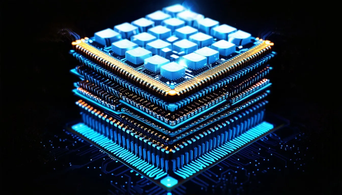
Processing-in-memory (PIM) architectures address this inefficiency by relocating computation directly into or adjacent to the memory arrays, thereby eliminating the need to shuttle data back and forth across the system bus. By embedding computational logic within the memory subsystem, PIM reduces the distance data must travel, which drastically lowers latency and energy consumption. This approach targets the root cause of the von Neumann hindrance by enabling the memory to perform specific operations on the data it stores before sending the results to the main processor. The implementation of PIM can take several forms, ranging from processing units placed on the same silicon die as the memory arrays to logic layers stacked vertically atop the memory using three-dimensional setup techniques. These architectures allow for high-bandwidth access to data because the computation occurs where the data resides, applying the internal parallelism intrinsic in memory structures. The reduction in data movement volume translates directly to lower power dissipation and higher overall system throughput, particularly for data-intensive applications that exhibit high spatial and temporal locality.
Near-memory processing is a specific implementation of this concept where compute units are placed physically close to the memory banks, often on the same interposer or package, without altering the internal structure of the memory cells themselves. This method utilizes advanced packaging technologies to shorten the physical distance between the logic and the memory, reducing the capacitance and resistance of the interconnects. While near-memory processing does not achieve the same level of energy efficiency as in-memory computing, it offers a practical compromise that allows for the use of standard memory manufacturing processes combined with mature logic fabrication nodes. This approach facilitates the connection of powerful processing elements that can handle complex logic sequences while still benefiting from significantly higher bandwidth compared to traditional system-level layouts. The tight coupling ensures that the latency penalty for accessing memory is minimized, allowing the compute units to operate on data streams with much higher efficiency than discrete processors. In-memory computing goes a step further by embedding the computation directly into the memory array, enabling operations such as matrix-vector multiplication to occur within the memory substrate itself.
This technique applies the physical properties of the memory circuitry to perform calculations, effectively transforming the memory array into a massive parallel computational engine. Digital in-memory computing utilizes standard CMOS logic gates integrated into the peripheral circuitry or within the array to perform precise Boolean or arithmetic operations on the data bits as they are accessed. This digital approach ensures high computational accuracy and reliability, though it typically incurs a higher area overhead compared to analog alternatives. By performing operations at the bit-level or word-level directly where the data is stored, digital in-memory computing eliminates the need to move data entirely for certain classes of algorithms, resulting in extreme energy efficiency for tasks like bit-logic operations, database searching, and encryption. Analog in-memory computing employs the physical characteristics of non-volatile memory devices to perform arithmetic operations during the read process, utilizing principles such as Ohm’s Law and Kirchhoff’s Law. In these architectures, the conductance of a memory cell is a synaptic weight, and the input voltage is the activation value.
When voltages are applied to the rows of a memory array, the current flowing through each cell is the product of the input voltage and the cell conductance, effectively performing a multiplication operation. The summation of these currents along the bit-lines completes the multiply-accumulate operation essential for neural network inference and training. This analog approach allows for the execution of massive matrix operations in a single time step, offering throughput that is orders of magnitude higher than digital processors while consuming minimal power. The primary challenge lies in the precision of the analog computation, as device variability and noise can affect the accuracy of the results. Three-dimensional stacked DRAM technologies, such as High Bandwidth Memory (HBM), have provided the physical foundation necessary to make practical PIM implementations a reality. These technologies stack multiple layers of memory dies vertically and connect them using Through-Silicon Vias (TSVs), which are vertical electrical connections that pass through the silicon wafer.
This vertical stacking dramatically increases the density of memory bandwidth available to the processor, providing terabytes per second of throughput. The presence of a logic base layer in HBM stacks offers a unique opportunity to integrate processing units directly alongside the memory cubes. Samsung’s Aquabolt-XL HBM-PIM exemplified this approach by working with AI processing units into the HBM2E stack, effectively placing programmable compute capabilities within the memory package. This configuration demonstrated that specific AI workloads could achieve up to double the performance while reducing energy consumption by approximately 70% compared to systems relying solely on a host GPU and standard HBM. The commercialization of PIM technologies has expanded beyond proprietary accelerator stacks to include programmable architectures that allow developers to execute custom code within the memory. UPMEM commercialized DRAM-based PIM chips that feature a general-purpose processing unit embedded within each memory rank.
These Processing Units are capable of executing standard C code and operate independently, accessing their local memory bank with extremely low latency. This architecture proved highly effective for data-intensive applications such as genomics and database acceleration, where the volume of data movement typically overwhelms the processor. By offloading simple filtering and comparison operations to the in-memory processors, the main CPU is relieved of the burden, and the system avoids moving petabytes of raw data across the main bus. SK Hynix furthered this development with their Accelerator-in-Memory (AiM) solution, which is based on HBM3 technology and designed specifically to enhance data processing efficiency for AI applications by connecting with processing logic directly into the memory buffer die. Performance benchmarks derived from these commercial implementations have validated the theoretical advantages of PIM across a variety of workloads. Tests involving graph processing algorithms, which typically suffer from poor locality due to random access patterns, have shown throughput improvements ranging from 2 to 5 times when utilizing PIM architectures.
Similarly, neural network inference tasks benefit from the massive parallelism offered by in-memory compute engines, with energy per operation reduced by a factor of 5 to 10 times compared to discrete GPU implementations. These gains stem from the elimination of data fetch overhead and the reduction of cache misses that plague traditional processors when handling large datasets. The ability to process data in place allows these systems to sustain high utilization rates of the memory bandwidth, ensuring that every bit transferred contributes directly to a computational result. Startups in the semiconductor industry have focused on using analog in-memory computing to target edge AI applications where power efficiency is primary and raw throughput is secondary to battery life. Companies like Mythic and TetraMem have developed chips that utilize flash memory or resistive RAM arrays to perform neural network inference entirely in the analog domain. These devices compete by offering orders of magnitude improvement in performance-per-watt compared to digital solutions, making them suitable for deployment in autonomous vehicles, drones, and smart sensors.
While analog approaches face challenges regarding precision and the need for extensive calibration to handle device mismatch, they offer a compelling path toward deploying complex AI models at the edge without the thermal constraints imposed by traditional processors. The focus on analog compute highlights a divergence in PIM strategies, with digital methods dominating data center applications requiring precision and analog methods capturing the low-power edge market. The realization of advanced PIM architectures relies heavily on sophisticated packaging techniques and semiconductor manufacturing capabilities that are currently dominated by a few major foundries. Through-Silicon Vias (TSVs) and silicon interposers are critical components that enable the dense vertical setup of logic and memory layers. The fabrication of these structures requires specialized equipment and processes that introduce dependencies on foundries with advanced 3D stacking capabilities. The materials used in appearing memory technologies present supply chain constraints.
Resistive RAM often relies on hafnium oxide, while Phase Change Memory utilizes chalcogenide glass materials. The sourcing and processing of these niche materials are less mature than the silicon supply chain, potentially limiting the adaptability of production volumes. As demand for PIM grows, the semiconductor industry must address these material and packaging limitations to ensure cost-effective mass production. Key physical limits regarding heat dissipation and signal integrity pose significant challenges to the continued miniaturization of compute-in-memory cells. As logic elements are integrated more tightly with memory arrays, the power density within the chip increases, making thermal management difficult. Unlike traditional chips, where the processor and memory are separate and can be cooled independently, a monolithic PIM chip generates heat within the memory substrate itself, which can degrade data retention times and device reliability.
Signal integrity also becomes a concern as feature sizes shrink and operating speeds increase, with crosstalk between adjacent interconnects potentially introducing errors in both data storage and computation. These physical constraints necessitate careful architectural design to balance computational density with thermal limits and noise margins. Variability in analog memory devices introduces significant noise into the calculation process, limiting the precision achievable with analog in-memory computing. The conductance of a resistive RAM cell can drift over time or vary due to manufacturing inconsistencies, leading to inaccuracies in the multiplication results. This lack of precision requires software-level compensation techniques, such as noise-aware training or periodic recalibration of the synaptic weights stored in the memory. While neural networks are inherently tolerant to some level of noise, maintaining acceptable accuracy for complex models demands rigorous control over device physics.

The trade-off between the energy efficiency of analog compute and the precision of digital arithmetic remains a central research topic, driving innovations in device engineering and circuit design to mitigate variability effects. Field-Programmable Gate Arrays (FPGA) have provided a reconfigurable alternative to monolithic PIM designs through near-memory processing solutions such as Xilinx Versal. These devices integrate programmable logic with high-bandwidth memory interfaces and network-on-chip fabrics that allow developers to implement custom hardware accelerators improved for specific data movement patterns. While FPGAs offer flexibility and rapid prototyping capabilities, they generally lack the density and energy efficiency of dedicated PIM designs. The overhead of programmable logic means that an FPGA implementation will consume more area and power per operation than a hardwired in-memory compute engine. Despite these inefficiencies, FPGAs serve as a valuable bridge technology, allowing system architects to experiment with near-memory algorithms before committing to the design of full custom ASICs.
The software stack required to enable the potential of PIM architectures must undergo a significant redesign to expose memory-side computation to the programmer and compiler. Traditional programming models assume a passive memory hierarchy where data is fetched to the CPU for processing. PIM requires new programming models that allow developers to explicitly offload kernels of computation to the processing units within the memory. Compilers must be capable of identifying data-intensive code regions and mapping them efficiently onto the PIM architecture while managing data coherence between the host processor and the in-memory units. Runtime systems need to handle task scheduling, load balancing, and synchronization across heterogeneous compute resources that are distributed throughout the memory hierarchy. The complexity of this software ecosystem is a substantial barrier to adoption, as legacy code cannot benefit from PIM without significant refactoring or sophisticated compiler automation.
Operating systems and memory managers must evolve to support heterogeneous memory-compute resources and active workload offloading transparently. The OS needs to be aware of the capabilities of different memory regions, distinguishing between standard DRAM and memory banks equipped with processing units. Virtualization mechanisms must extend to allow virtual machines to allocate and utilize PIM resources securely without interfering with one another. Memory management policies should fine-tune for data locality by keeping data close to the PIM units that are processing it, reducing the need for expensive transfers across the NUMA domains. This deep setup between the OS and hardware is essential for achieving high utilization rates in systems containing diverse types of accelerators. Existing performance metrics, such as FLOPS, bandwidth, and latency, are insufficient to accurately evaluate the capabilities of PIM architectures.
FLOPS measure only the computational rate of the processing unit, while ignoring the cost of data movement, which is precisely what PIM aims to improve. New Key Performance Indicators (KPIs) are necessary, such as energy per operation, total data movement volume, and compute-to-memory ratio. These metrics provide a more holistic view of system efficiency by quantifying how much work is done for every joule of energy consumed or every byte of data transferred. The industry needs standardized benchmarks that reflect real-world data movement patterns rather than synthetic compute-bound workloads that fit entirely within the CPU cache. Only through accurate measurement can the true benefits of PIM be assessed and compared against traditional architectures. System-level efficiency metrics such as operations per joule per byte moved become critical for evaluating large-scale data center deployments
Economic pressure to reduce operational expenses drives the adoption of architectures that minimize data transfer overhead. As workloads become increasingly memory-bound, the ability to perform operations directly on data with minimal movement offers a direct path to lowering costs. Benchmark suites must evolve to include graph analytics, genomic sequencing, and large-scale neural network training, all of which stress the memory subsystem heavily. These benchmarks will highlight the scenarios where PIM provides decisive advantages over conventional systems. Superintelligence systems will demand extreme efficiency in data handling to scale beyond current computational limits. The cognitive processes associated with superintelligence, involving reasoning, learning, and planning over vast knowledge bases, require the manipulation of exabytes of data in real-time. Traditional architectures would collapse under the energy and latency requirements of moving such massive amounts of data between disjointed components.
PIM enables massive parallelism with minimal data movement, aligning perfectly with the memory-bound nature of these large-scale reasoning tasks. By distributing intelligence throughout the memory hierarchy, a superintelligent system can achieve the necessary throughput to maintain coherence across its entire knowledge base without being throttled by communication constraints. In-memory computing will support continuous, low-latency inference for large workloads, which is critical for real-time autonomous decision-making in superintelligent agents. An agent interacting with the physical world must process high-bandwidth sensory streams and update its internal state instantaneously to respond effectively. The latency incurred by shuttling sensor data from acquisition buffers to a distant processor creates an unacceptable delay in time-critical applications. In-memory processing allows sensory inputs to be processed immediately upon arrival at the memory buffer, extracting features and triggering actions with minimal delay.
This capability is essential for superintelligent systems that must operate with reaction times faster than biological organisms in adaptive environments. The connection of optical interconnects with PIM architectures will enable ultra-low-latency communication between memory-compute units for future systems. As systems scale to millions of processing cores, electrical interconnects become a limiting factor due to resistance, capacitance, and heat generation. Optical communication offers high bandwidth and low attenuation over longer distances, making it ideal for linking separate PIM modules into a cohesive superintelligent fabric. Combining optical I/O with in-memory compute allows for the creation of disaggregated systems where memory-compute nodes communicate at light speed, effectively creating a single global brain distributed across a physical substrate. This synergy addresses both the intra-chip data movement issues via PIM and the inter-chip communication issues via photonics.
The development of universal memory technologies that combine speed, density, non-volatility, and compute capability will facilitate these advanced architectures. Current memory hierarchies involve a trade-off between speed (SRAM), density (DRAM), and non-volatility (Flash). A universal memory that matches DRAM speed while retaining data without power and supporting in-memory computation would eliminate the need for complex tiered storage systems. Such a technology would drastically simplify system architecture and reduce the energy wasted by constantly moving data between volatile and non-volatile layers. Research into ferroelectric field-effect transistors (FeFET) and other novel devices aims to realize this universal memory goal, providing the ideal substrate for persistent superintelligent cognition. Scalable compiler frameworks will automatically partition workloads between host processors and PIM units to manage complex superintelligent tasks without manual intervention.
Given the complexity of software for superintelligence, programmers cannot be expected to manually improve every kernel for specific hardware configurations. Compilers must analyze data dependencies and access patterns to decide which portions of a graph algorithm or neural network should execute on the CPU versus the PIM units. This automated partitioning ensures that the heterogeneous resources of the system are utilized optimally, adapting dynamically to changing workload characteristics. The compiler acts as an intelligent scheduler that maximizes throughput while minimizing energy consumption across the entire hardware stack. PIM converges with neuromorphic computing, where memory and computation co-location mimics biological neural networks. The human brain operates efficiently because synapses store weights and perform signal connection simultaneously without separating memory from processing.

Neuromorphic chips implement this principle using arrays of artificial neurons and synapses, which are fundamentally similar to analog in-memory computing architectures. This convergence suggests that the path to artificial general intelligence and superintelligence lies in moving away from the von Neumann framework toward brain-inspired architectures where processing is common throughout the memory fabric. The adaptability of such neuromorphic PIM systems allows them to support the massive connectivity required for human-level reasoning. Synergies with quantum computing memory interfaces will arise where low-energy data handling is essential. Quantum computers operate at cryogenic temperatures and face severe restrictions on heat dissipation and wiring bandwidth. Classical control systems for quantum processors generate vast amounts of data that must be processed to correct errors and interpret quantum states.
Placing PIM units within the cryostat or at the edge of the quantum chassis allows for immediate processing of control signals with minimal thermal load. Efficient data handling provided by PIM is critical for scaling quantum computers to useful qubit counts, as it reduces the I/O constraint that currently limits feedback loops in quantum error correction. The intersection of quantum computing and superintelligent classical control will likely rely heavily on advanced memory-centric architectures.