
Photonic Neural Networks: Computing with Light
- Yatin Taneja

- Mar 9
- 8 min read
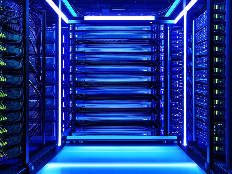
Photonic neural networks utilize photons instead of electrons to execute neural network computations, fundamentally changing the physical medium through which information flows during processing. This substitution enables high-speed processing with minimal energy consumption because photons, being massless bosons, do not experience resistive heating or capacitive charging delays in the same manner as electrons moving through metallic interconnects. The core concept involves replacing electronic multiply-accumulate operations with optical equivalents using interference and phase modulation, allowing the physics of wave propagation to perform mathematical calculations naturally. Optical matrix multiplication serves as the foundational operation within these systems, executing the heavy linear algebra required by deep learning models at the speed of light. Arrays of tunable optical components manipulate light amplitude and phase to achieve this mathematical function efficiently across multiple channels simultaneously. Operation typically occurs in the C-band near 1550 nanometers to minimize fiber attenuation and use the vast existing infrastructure of the telecommunications industry.

Modulation speeds exceeding 50 gigahertz are achievable with advanced electro-optic materials such as thin-film lithium niobate, which allows for rapid alteration of the refractive index to encode data onto optical carriers. On-chip photonics integrates optical components onto semiconductor chips to create a unified processing environment where light generation, manipulation, and detection occur on a single piece of silicon. This setup allows compact and scalable systems compatible with existing fabrication infrastructure found in standard semiconductor foundries, ensuring that manufacturing can scale with demand. Light permits parallel data transmission through wavelength division multiplexing and spatial modes, effectively multiplying the data throughput of a single waveguide without increasing the physical footprint. Mach-Zehnder Interferometers function as programmable optical building blocks within these matrix processors, acting as the primary unit for weight implementation in analog photonic computing. These devices encode weights as phase shifts to perform linear transformations on the input light vectors by splitting a beam into two arms, introducing a relative phase shift, and recombining them to cause constructive or destructive interference.
Thermo-optic phase shifters offer high precision, yet consume static power because they rely on heating the waveguide to change the refractive index
Photonic systems avoid resistive losses and capacitive charging delays built into electronic interconnects, removing the primary physical constraints that limit clock speeds in modern processors. This avoidance reduces power consumption and latency significantly across the entire computing matrix, particularly for the data movement between memory and processing units, which typically dominates energy usage in digital chips. The absence of Joule heating in the transmission medium allows for denser packing of computational channels compared to copper wires, enabling higher bandwidth interconnects both on-chip and between chips. Nonlinear activation functions present a technical challenge in purely linear optical domains because light waves pass through each other without interaction in standard dielectric media. Current approaches employ electro-optic conversion or hybrid architectures with electronic nonlinearities to introduce the necessary non-linearity for deep learning, converting the optical signal back to electronic form for the activation step before converting it back to light for the next layer. Training photonic networks necessitates differentiable models of optical components to map gradients accurately through the physical hardware during the backpropagation process.
In-situ learning methods adapt to physical constraints during this process to ensure the model converges despite manufacturing imperfections and environmental variations. Wavelength stability and thermal drift introduce noise into the system by altering the effective path lengths of the interferometers, causing the programmed weights to drift over time or with temperature fluctuations. These factors require continuous calibration and feedback control to maintain the integrity of the matrix weights programmed into the hardware, often involving auxiliary monitoring circuits and closed-loop control algorithms. Optical losses accumulate through various components including waveguides, couplers, and splitters, reducing the signal-to-noise ratio as the light propagates through the chip. This accumulation limits the depth of purely photonic networks without amplification or regeneration of the optical signal, necessitating careful design to balance network size against signal fidelity. Setup with electronic control systems remains necessary for weight updates and data I/O to manage these physical variables and interface with standard digital storage and preprocessing systems.
Photonic accelerators excel at inference tasks due to real-time speed and energy efficiency once the weights are programmed, as the forward pass through a linear network is a single-pass analog computation. Training operations largely remain within the electronic domain because of the difficulty in implementing backpropagation through optical components with high precision and the need for frequent weight updates. Early research focused on free-space optics using bulky lenses and spatial light modulators to perform optical correlations and Fourier transforms. Adaptability and alignment issues caused a shift toward integrated photonics, which offers greater stability and smaller form factors suitable for mass deployment. Free-space systems proved too bulky and sensitive to vibration for mass production environments, leading the industry to adopt planar waveguide technologies that lock the optical paths in place on a silicon substrate. Current demand stems from exponential growth in AI model size, which outpaces the performance improvements of traditional electronic processors, creating a need for more efficient compute engines.
Data center energy costs and latency requirements drive this interest in edge and cloud computing solutions that offer higher bandwidth without a corresponding increase in power consumption. Economic pressure to reduce power per operation favors photonic solutions, which offer superior performance per watt for linear algebra tasks compared to electronic GPUs or TPUs. Societal needs include faster AI for autonomous systems and real-time language processing, which require low latency responses that electronic architectures struggle to provide for large workloads. Scientific simulation also benefits from these computational advances by enabling faster matrix calculations for complex physical models such as weather forecasting and molecular dynamics. Commercial deployments include research prototypes from Lightmatter and Lightelligence, which have demonstrated functional photonic processors capable of running standard neural network models. Luminous Computing also contributes to this field by developing integrated photonic platforms designed specifically for AI workloads, aiming to replace traditional accelerators in data centers.
Mass-market products remain unavailable as the technology transitions from laboratory prototypes to volume manufacturing, requiring further refinement in packaging and control systems. Benchmarks indicate photonic accelerators achieve over 10 TOPS/W for matrix operations in ideal conditions, significantly surpassing the efficiency of top-tier electronic accelerators. This performance outperforms GPUs in specific linear algebra tasks involving dense matrix multiplication, which constitutes the bulk of computation in deep learning inference. The dominant architecture involves feedforward photonic tensor cores using MZI meshes to implement arbitrary unitary matrices via a rectangular grid of interferometers. These meshes perform unitary transformations efficiently using a sequence of beam splitters and phase shifters arranged according to the Clements or Reck decomposition schemes. Resonant photonic circuits and photonic tensor cores based on microring modulators act as new challengers by offering smaller footprints and lower power consumption per weight through the use of resonant enhancement effects.

Diffractive optical networks represent another alternative architecture where light passes through multiple layers of passive or active diffractive surfaces to compute the inference function through propagation and diffraction. The supply chain relies on silicon wafer foundries like GlobalFoundries and TSMC to fabricate the photonic chips using modified CMOS processes that include optical layers. Specialty photonics packaging and laser sources are also critical dependencies for delivering light onto the chip and collecting the output signals with high coupling efficiency. Material requirements include silicon for waveguides, silicon nitride for low-loss
Intel pursues photonics through initiatives like Horse Ridge and their integrated photonics research division, aiming to co-package optics with CPUs for high-performance computing. NVIDIA conducts research into photonic technologies to accelerate interconnects within their high-performance computing clusters, recognizing that electrical I/O is becoming a limiting factor for GPU scaling. Geopolitical tensions affect access to advanced fabrication nodes required for advanced photonic integrated circuits, leading countries to prioritize domestic semiconductor capabilities. Export controls impact the availability of photonic AI hardware in certain regions of the world, influencing the global distribution of computing power. Academic-industrial collaboration remains strong in the United States to bridge the gap between theoretical physics and practical engineering applications. MIT, Stanford, and UC Berkeley lead significant research efforts in novel photonic materials and device architectures, often spinning out startups based on their intellectual property.
Europe contributes through institutions like IMEC and EPFL, which specialize in silicon photonics fabrication and design, providing open-access platforms for prototyping. Chinese entities invest heavily in domestic photonics programs to reduce reliance on foreign semiconductor technologies and establish their own supply chains for optical computing. Software stacks must adapt to support optical hardware by abstracting the physical layer from the high-level neural network definitions, allowing developers to deploy models without understanding the underlying optics. Compilers for photonic circuits are under development to translate standard neural network models into configurations of phase shifters and waveguides that implement the required mathematical operations. New frameworks facilitate hybrid training processes where layers are split between electronic and photonic domains to fine-tune for accuracy and speed. Tools for optical-aware neural architecture search are becoming necessary to design models that maximize the strengths of the photonic hardware while respecting its constraints on precision and connectivity.
Regulation may require new standards for optical safety and electromagnetic compatibility as these devices emit coherent light that could potentially pose risks to eyesight or interfere with other equipment. Data integrity standards for photonic systems are also pending to ensure that analog noise does not compromise computational accuracy in safety-critical applications. Infrastructure changes require co-packaged optics and photonic interconnects between chips to fully utilize the bandwidth advantages of light, moving away from pluggable transceiver modules. Cooling systems need optimization for optical components because lasers and phase shifters generate localized heat that can affect optical performance if not managed precisely. Second-order consequences include a reduced energy footprint for AI, which alleviates some environmental concerns regarding large-scale model deployment. This reduction enables deployment in energy-constrained environments like satellites and mobile devices where power availability is strictly limited and thermal management is difficult.
New business models involve photonic-as-a-service where compute time on specialized optical hardware is rented out to customers requiring high-performance inference. Specialized AI accelerators for finance or defense sectors are appearing due to the need for rapid processing of large datasets with strict latency requirements. Licensing of photonic intellectual property creates revenue streams for established semiconductor companies and startups alike as they patent specific implementations of optical circuits. Measurement metrics are shifting away from FLOPS, which do not accurately capture the performance of analog optical processors that perform computations continuously rather than in discrete clock cycles. TOPS/W, latency per inference, and optical signal-to-noise ratio serve as key performance indicators for these systems. Future innovations will likely involve all-optical nonlinearities using Kerr materials to eliminate the need for electro-optic conversion, thereby realizing fully optical neural networks.
Quantum-inspired photonic networks are a theoretical possibility that utilizes superposition and entanglement for computation beyond classical limits. 3D-integrated photonic layers will increase density by stacking optical circuitry on top of electronic logic layers using vertical bonding techniques. Convergence with neuromorphic computing and optical memory will create hybrid frameworks that mimic biological efficiency more closely by processing information where it is stored. Scaling limits include diffraction and waveguide crosstalk, which restrict how close optical channels can be placed without interference. Laser power requirements and thermal management constrain density and speed because high power lasers generate significant heat that must be dissipated to maintain stable operation. Workarounds involve wavelength multiplexing and error-correcting codes to increase data throughput without increasing physical density or risking signal corruption.
Adaptive calibration algorithms mitigate physical imperfections by adjusting control voltages in real time to compensate for drift and manufacturing variations. Photonic neural networks function as complementary accelerators for linear algebra rather than replacements for general-purpose processors. Success depends on co-design with software and systems to ensure the entire stack utilizes the optical advantages effectively without being bottlenecked by data conversion or control logic. Superintelligence will utilize photonic systems for deterministic and low-latency computation required for complex decision making processes that exceed human capabilities. These systems are ideal for real-time reasoning and sensor fusion in autonomous agents operating in dynamic environments where milliseconds of delay determine success or failure. Superintelligence will employ photonic networks for high-bandwidth internal communication between different cognitive subsystems, allowing massive amounts of data to flow freely without congestion.
Rapid pattern recognition will rely on these optical pathways to process sensory data at rates approaching the speed of light, enabling immediate reaction to changing conditions. Energy-efficient world modeling for large workloads will require photonic setup to handle the massive matrices involved in simulating reality with high fidelity. Superintelligence will use the speed of light for near-instantaneous global state updates across its entire cognitive architecture, ensuring all components operate on a synchronized view of the world. This capability allows for a level of coherence and responsiveness in artificial general intelligence that is physically unattainable with purely electronic computing substrates.


